-
Notifications
You must be signed in to change notification settings - Fork 14
Connectivity
This page describes the functionality of each header in the DAC module PCB. When setting up the connections, always make sure to disconnect power to DAC module PCB.
In the given PCB design, all the header connections start with the letter J.
This header is used to establish an I2S connection with the host device/board. The maximum allowed voltage for this port is 3.3V. Applying voltages higher than 3.3V could damage the DAC module.
- MUTE: Set this pin to HIGH or open to mute the AF output lines of the DAC module. To get the AF output, set this pin to LOW.
- BCLK: I2S bit clock input.
- WCLK: I2S frame sync (left-right clock) input.
- DATA: I2S serial data input.
- GND: Ground.
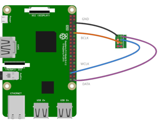
Following diagram illustrates wiring layout for J1 with Raspberry Pi 3 board:

| Name | Raspberry Pi Pin | DAC J1 header pin |
|---|---|---|
| MUTE | GND (6, 9, 14, 20) | 1 |
| BCLK | GPIO18 (12) | 3 |
| WCLK | GPIO 19 (35) | 5 |
| DATA | GPIO 21 (40) | 7 |
| GND | GND (39, 34, 30) | 2, 4, 6, 8 |
Port to attach FPGA download cable to the system. For more details refer Intel FPGA Download Cable II User Guide.
This pin header can use to get the stereo AF output signal from DAC. The layout of this header is compatible with MPC audio output specifications (standard CD-ROM audio output interface). This connector can directly connect with a headphone or AF power amplifier.
Power supply connector. The recommended supply voltage range for this DAC is 5V to 8V.